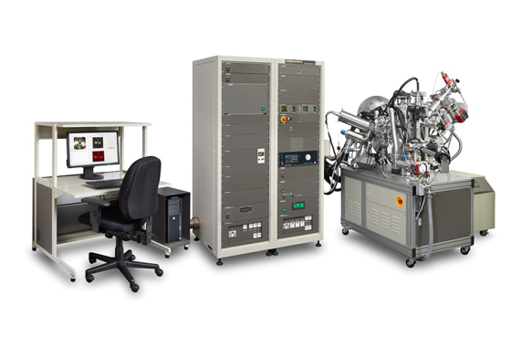
Test and Failure Analysis

Auger Electron Spectroscopy (AES)

Equipment model:PHI-710
Focusing on various energy storage business needs, TIES strives to develop into a comprehensive, market-oriented R&D enterprise that integrates testing analysis, failure analysis, qualification certification, technology development, engineering amplification, intelligent manufacturing, high-value information services, and high-end training. Contact us

Technical Parameters

  1. Stable Schottky field emission source operating at 1-25 kV;

  2. Secondary electron imaging resolution up to 4096×4096 pixels;

  3. Spatial resolution: 8 nm;

  4. Collection depth: 5-75 Å;

  5. Elemental detection limit: 0.1 atom %;

  6. Information collected: Elements (Li~U) and partial chemical states;


Application Range

Used for analyzing the elemental (including partial chemical states) composition at nanometer depths of solid material surfaces. It allows observation of nanometer-scale topographies and compositional characterization. It can analyze the uniform surface composition of raw materials (such as powder particles, sheets, etc.) as well as analyze surface defects of materials or specific products such as pollution, corrosion, doping, adsorption, impurity segregation, etc. It also possesses depth profiling capabilities to characterize passivation layers, doping depths, nanometer-scale multilayer structures, and more.


Related Recommendations

Scanning Electron Microscope (SEM)
Technical ParametersSecondary Electron Resolution: 0.8 nm (acceleration voltage 15 kV) (standard mode, not in any deceleration mode)1.1 nm (acceleration voltage 1 kV) (deceleration mode)Magnification: 20 to 1000k Acceleration Voltage: 20-1000kElectronic Displacement: ±12μm (WD=8mm)Aperture: 4-hole objective movable aperture system: built-in self-cleaning device (aperture 30, 50, 50, 100μm)Detectors: Lower and Upper secondary electron detectors, Upper filtered backscatter detectorSignal Selection: Secondary electron image, Backscattered electron image, Mixed imageRapid Sample Exchange System: 100mm diameter large sample exchange chamber, sample exchange time is 30 secondsVacuum Transfer System: Hitachi original vacuum transfer systemEnergy Spectrometer: Bruker 60mm2 energy spectrometerApplication RangeThe deceleration function of acceleration voltage has a series of advantages such as shorter wavelength, smaller aberrations, and higher resolution. It can reduce sample damage while obtaining low-voltage high-resolution images.The SE/BSE signal reception function in proportion. The electron microscope is equipped with Lower and Upper secondary electron detectors, and a Upper filtered backscatter probe. By changing the voltage of the internal transformer electrode of the lens, the detector can capture secondary electrons and backscattered electrons, mix them in any proportion (100 levels), achieve optimal contrast observation, suppress charge and edge effects, and obtain the best contrast SEM image.

Detail

X-ray Photoelectron Spectroscopy (XPS)
Technical ParametersEnergy Resolution: FWHM of Ag3d5/2 peak < 0.48eV; FWHM of O=C-O peak in C1s spectrum < 0.82eVMinimum x-ray Beam Spot Size: <10.0μm (x-axis); <10.0μm (y-axis)Maximum Beam Current of Ar Ion Sputter Gun: >5.0μA @5kVDifferential Pressure of Ar Ion/C60 Ion Sputter Gun: < 6.7x10⁻⁶ Pa (5x10⁻⁸Torr)Maximum Current of Ar Gas Cluster Ion Gun: >40nA @ 20kVMinimum Beam Spot Size of Ar Gas Cluster Ion: 500 μm @ 20 kVThermal Performance of Sample Stage: -140°C to 800°CApplication RangeInorganic compounds, alloys, polymers, energy batteries, surface defects (corrosion, foreign substances, contamination, uneven distribution, etc.), surface multilayer films, etc.

Detail

CopyRight © 2024 Tianmu Lake Institute of Advanced Energy Storage Technologies All Rights Reserved. 苏ICP备18030956号-1